
Our Equipment
Film Growth
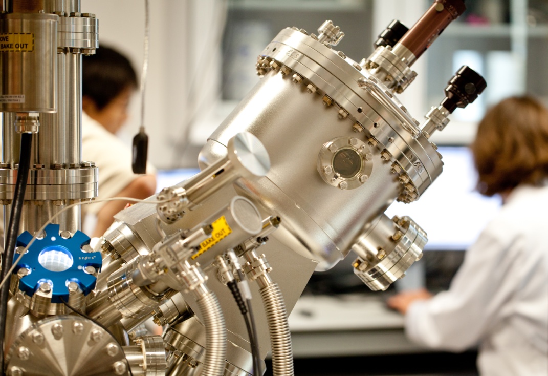
 The Device Materials Group has extensive facilities for the fabrication of thin films and hetero-structures of many different materials. Films are produced using magnetron sputtering (DC or RF) or pulsed laser deposition. The DMG film growth fleet consists of more than a dozen UHV deposition systems and three high power KrF excimer lasers.
Our sputtering and laser ablation systems are built for great flexibility, allowing easy change of targets and adjustment of growth parameters. Films requiring up to six different targets can be produced in one deposition sequence, facilitating the growth of complex device structures and multilayers. Use of different gases (including Ar, O2, and N2) enables us to grow films of pure elements, alloys and compounds. Substrate temperature can be controlled using built-in heaters (e.g. for epitaxial film growth) and cold-stages (as needed to produce amorphous films). Multiple target holders, and rotating sample supports with computer controlled stepper motors enable extremely accurate control of film thickness and composition (e.g. for combinatorial studies). In-situ cleaning of sample surfaces and interfaces can be carried out with either a hydrogen or argon ion gun. In-situ RHEED characterisation allows layer by layer growth control for PLD grown films.
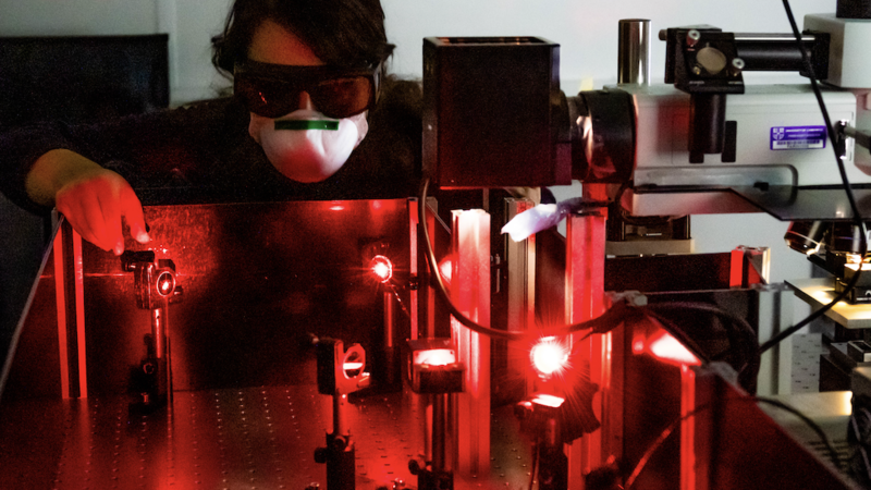
Optical Characterization
We develop the ultra-concentration of light trapped inside plasmonic nanocavities into an innovative fast methodology for studying real-time movement of individual atoms that underpins the new generation of memory nano-devices. Ongoing research topics include Dark Field, surface-enhanced Raman and Photoluminescence spectroscopy.
Physical Properties Measurement
The device materials group has a wide array of facilities for electrical and magnetic characterization of thin films and devices, and work is focused on 4 key areas – interplay of Superconductivity and ferromagnetism, multiferroics, solar cells and functional thin films.
 Custom made dip probes are used for resistance measurements and characterisation of Josephson Junctions and superconducting tunnel junctions to temperatures down to 0.3 K. Lock-in amplifiers connected to these dip probes enable ultra-low noise measurements. Additionally, Heliox probes from Cryogenic ltd. allow electrical measurements down to 0.3 K in the presence of magnetic field of 1 Tesla. The Cryofree high field (up to 9 Tesla) measurement system has capabilities for being used in various modes such as VSM, resistivity, Hall AC susceptibility, dilatometry, and can operate in the temperature range of 0.3 K to 650 K. Both pieces of equipment from Cryogenic ltd. operate in a helium closed cycle mechanism. A separate VSM usually dedicated for room temperature magnetic measurements gives a sensitivity of 1 μemu and can also be cooled to liquid helium temperatures.